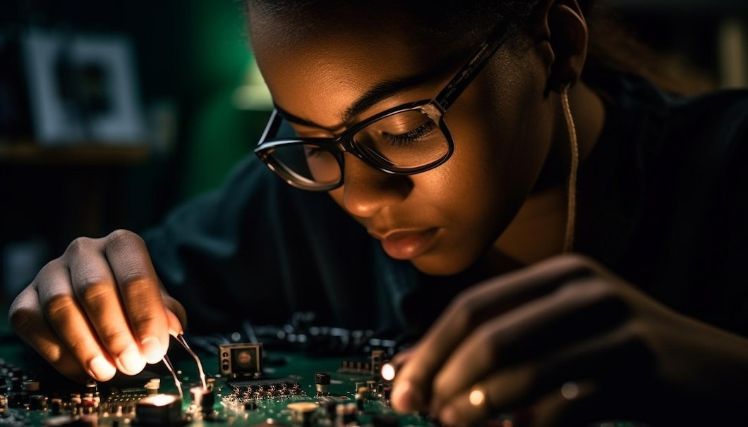
Printed Circuit Boards (PCBs) are the backbone of almost all modern electronic devices, from smartphones to spacecraft. PCB design is a critical step in the electronics development process; even small PCB design mistakes can lead to significant issues.
Common PCB Design Mistakes and How to Avoid Them
To help you create efficient and reliable PCBs, here are the top 10 common PCB design mistakes and how to avoid them:
1. Inadequate Component Placement

Placing components too closely or far apart can lead to issues such as signal interference and heat dissipation problems. To avoid this, carefully plan the component placement, follow the design guidelines provided by the components’ manufacturers, and use PCB design software to check design rules.
2. Ignoring Thermal Management
Overheating is a major problem in electronics. Neglecting thermal management can result in component failures and reduced lifespan. Ensure your PCB design includes proper heat sinks, vias, and thermal relief patterns. Use simulation tools to analyze and address thermal issues.
3. Inadequate Ground and Power Planes
Poor grounding can introduce noise and signal integrity problems. Always have a solid ground plane and carefully manage power distribution. If necessary, implement multiple ground and power planes and use copper pours to ensure a stable power supply and ground reference.
4. Trace Routing PCB Design Mistakes
Routing traces haphazardly or with incorrect dimensions can lead to signal integrity issues and electromagnetic interference (EMI). Follow signal integrity guidelines, maintain consistent trace widths and spacing, and use controlled impedance routing when necessary.
5. Neglecting EMI/EMC Considerations
Electromagnetic interference (EMI) can affect both the functionality of your PCB and nearby electronic devices. To mitigate EMI, use proper grounding techniques, add EMI shielding, and pay attention to signal routing to minimize loop areas.
6. Inadequate Design for Manufacturability (DFM)
Ignoring DFM can result in costly and time-consuming production issues. Ensure that your design complies with PCB fabrication and assembly rules. This includes appropriate pad sizes, spacing, and clear silkscreen markings.
7. Improper Handling of High-Speed Signals
High-speed signals are particularly sensitive to impedance, reflections, and crosstalk. Pay close attention to trace lengths, differential pair routing, and termination techniques. Implement length matching and avoid 90-degree corners in traces.
8. Overlooking Component Footprint Errors
Component footprints must match the actual components. Double-check component footprints to avoid soldering and assembly issues. Use libraries from reputable sources or create custom footprints based on the component datasheets.
9. Inadequate Documentation

Complete and accurate documentation is crucial for the manufacturing and maintenance of your PCB. Provide a comprehensive bill of materials (BOM), assembly drawings, and detailed design files. Well-documented designs are more likely to be assembled correctly and serviced efficiently.
10. Lack of Testing and Prototyping
Skipping the testing phase can lead to costly errors that are difficult to rectify in the final product. Prototype your PCB design to uncover and address potential issues early in development. Use tools like oscilloscopes and logic analyzers to verify functionality.
Also Read: Hardware Design Services: Paving the Way for Innovation and Excellence
Avoiding these common PCB design mistakes requires knowledge, attention to detail, and advanced PCB design software. Continuous learning and staying updated on industry best practices and standards are essential for creating reliable and efficient PCBs.
Additionally, seeking peer reviews and expert feedback on your designs can help identify and rectify potential issues before they become costly problems in production. By taking these precautions and adhering to best practices, you can develop high-quality PCBs that perform as intended and have a longer lifespan, saving time and resources in the long run.
